%2540Zen2%2540Rome%2540EPYC_7702_ES%25402S1404E2VJUG5_BB_ES_DSCx6_IOD_top_metal%25405x.jpg.webp)
Flip chip, also known as controlled collapse chip connection or its abbreviation, C4,[1] is a method for interconnecting dies such as semiconductor devices, IC chips, integrated passive devices and microelectromechanical systems (MEMS), to external circuitry with solder bumps that have been deposited onto the chip pads. The technique was developed by General Electric's Light Military Electronics Department, Utica, New York.[2] The solder bumps are deposited on the chip pads on the top side of the wafer during the final wafer processing step. In order to mount the chip to external circuitry (e.g., a circuit board or another chip or wafer), it is flipped over so that its top side faces down, and aligned so that its pads align with matching pads on the external circuit, and then the solder is reflowed to complete the interconnect. This is in contrast to wire bonding, in which the chip is mounted upright and fine wires are welded onto the chip pads and lead frame contacts to interconnect the chip pads to external circuitry.[3]
Process steps
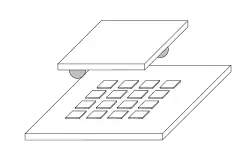
- Integrated circuits are created on the wafer.
- Pads are metallized on the surface of the chips.
- A solder ball is deposited on each of the pads, in a process called wafer bumping
- Chips are cut.
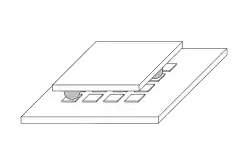
- Chips are flipped and positioned so that the solder balls are facing the connectors on the external circuitry.
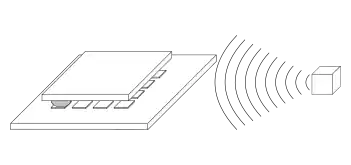
- Solder balls are then remelted (typically using hot air reflow).
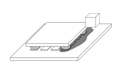
- Mounted chip is "underfilled" using a (capillary, shown here) electrically-insulating adhesive.[4][5][6][7]
Comparison of mounting technologies
Wire bonding/thermosonic bonding

In typical semiconductor fabrication systems, chips are built up in large numbers on a single large wafer of semiconductor material, typically silicon. The individual chips are patterned with small pads of metal near their edges that serve as the connections to an eventual mechanical carrier. The chips are then cut out of the wafer and attached to their carriers, typically via wire bonding such as thermosonic bonding. These wires eventually lead to pins on the outside of the carriers, which are attached to the rest of the circuitry making up the electronic system.
Flip chip

Processing a flip chip is similar to conventional IC fabrication, with a few additional steps.[8] Near the end of the manufacturing process, the attachment pads are metalized to make them more receptive to solder. This typically consists of several treatments. A small dot of solder is then deposited on each metalized pad. The chips are then cut out of the wafer as normal.
To attach the flip chip into a circuit, the chip is inverted to bring the solder dots down onto connectors on the underlying electronics or circuit board. The solder is then re-melted to produce an electrical connection, typically using a thermosonic bonding or alternatively reflow solder process.[9]
This also leaves a small space between the chip's circuitry and the underlying mounting. In many cases an electrically-insulating adhesive is then "underfilled" to provide a stronger mechanical connection, provide a heat bridge, and to ensure the solder joints are not stressed due to differential heating of the chip and the rest of the system. The underfill distributes the thermal expansion mismatch between the chip and the board, preventing stress concentration in the solder joints which would lead to premature failure.[10]
Solder balls can be mounted on the chips by separately making the balls and then attaching them to the chips by using a vacuum pick up device to pick up the balls and then placing them into a chip with flux applied on contact pads for the balls, or by electroplating in which seed metals are first deposited onto a wafer with the chips to be bumped. This allows the solder to adhere to the contact pads of the chips during the electroplating process. The seed metals are alloys and are deposited by sputtering onto the wafer with the chips to be bumped. A photoresist mask is used to only deposit the seed metal on top of the contact pads of the chips. The wafer then undergoes electroplating, and the photoresist layer is removed or stripped. Then the solder on the chips undergoes solder reflow to form the bumps into their final shape. This entire process is known as wafer bumping. Solder balls are often 75 to 500 microns in diameter.[11][12]
In 2008, High-speed mounting methods evolved through a cooperation between Reel Service Ltd. and Siemens AG in the development of a high speed mounting tape known as 'MicroTape'. By adding a tape-and-reel process into the assembly methodology, placement at high speed is possible, achieving a 99.90% pick rate and a placement rate of 21,000 cph (components per hour), using standard PCB assembly equipment.
Tape-automated bonding
Tape-automated bonding (TAB) was developed for connecting dies with thermocompression or thermosonic bonding to a flexible substrate including from one to three conductive layers. Also with TAB it is possible to connect die pins all at the same time as with the soldering based flip chip mounting. Originally TAB could produce finer pitch interconnections compared to flip chip, but with the development of the flip chip this advantage has diminished and has kept TAB to be a specialized interconnection technique of display drivers or similar requiring specific TAB compliant roll-to-roll (R2R, reel-to-reel) like assembly system.
Advantages
The resulting completed flip chip assembly is much smaller than a traditional carrier-based system; the chip sits directly on the circuit board, and is much smaller than the carrier both in area and height. The short wires greatly reduce inductance, allowing higher-speed signals, and also conduct heat better.
Disadvantages
Flip chips have several disadvantages.
The lack of a carrier means they are not suitable for easy replacement, or unaided manual installation. They also require very flat mounting surfaces, which is not always easy to arrange, or sometimes difficult to maintain as the boards heat and cool. This limits the maximum device size.
Also, the short connections are very stiff, so the thermal expansion of the chip must be matched to the supporting board or the connections can crack.[13] The underfill material acts as an intermediate between the difference in CTE of the chip and board.
History
The process was originally introduced commercially by IBM in the 1960s for individual transistors and diodes packaged for use in their mainframe systems.[14]
Alternatives
Since the flip chip's introduction a number of alternatives to the solder bumps have been introduced, including gold balls or molded studs, electrically conductive polymer and the "plated bump" process that removes an insulating plating by chemical means. Flip chips have recently gained popularity among manufacturers of cell phones and other small electronics where the size savings are valuable.
See also
- Flip-Chip modules – Digital Equipment Corporation trademarked version
- Solid Logic Technology
- IBM 3081
- Hybrid pixel detector
References
- ↑ E. J. Rymaszewski, J. L. Walsh, and G. W. Leehan, "Semiconductor Logic Technology in IBM", IBM Journal of Research and Development, 25, no. 5 (September 1981): 605.
- ↑ Filter Center, Aviation Week & Space Technology, September 23, 1963, v. 79, no. 13, p. 96.
- ↑ Peter Elenius and Lee Levine, Chip Scale Review. "Comparing Flip-Chip and Wire-Bond Interconnection Technologies". July/August 2000. Retrieved July 30, 2015.
- ↑ "BGA Underfill for COTS Ruggedization". NASA. 2019.
- ↑ "Underfill revisited: How a decades-old technique enables smaller, more durable PCBs". 2011.
- ↑ "Underfill".
- ↑ "Underfill Applications, Materials & Methods". 2019.
- ↑ George Riley, Flipchips.com. “Solder Bump Flip Chip.” November 2000. Retrieved July 30, 2015.
- ↑ https://www.analog.com/media/en/technical-documentation/application-notes/AN-617.pdf
- ↑ Venkat Nandivada. "Enhance Electronic Performance with Epoxy Compounds". Design World. 2013.
- ↑ https://sst.semiconductor-digest.com/2001/07/the-back-end-process-step-7-solder-bumping-step-by-step/
- ↑ "Flip Chip—The Bumping Processes". Integrated Circuit Packaging, Assembly and Interconnections. 2007. pp. 143–167. doi:10.1007/0-387-33913-2_10. ISBN 978-0-387-28153-7.
- ↑ Demerjian, Charlie (2008-12-17), Nvidia chips show underfill problems, The Inquirer, archived from the original on July 21, 2009, retrieved 2009-01-30
{{citation}}: CS1 maint: unfit URL (link) - ↑ George Riley, Introduction to Flip Chip: What, Why, How, Flipchips.com October 2000.
External links
- Amkor Flip Chip Technology: CSP (fcCSP), BGA (FCBGA), FlipStack® CSP
- Shirriff, Ken (March 2021). "Strange chip: Teardown of a vintage IBM token ring controller".


