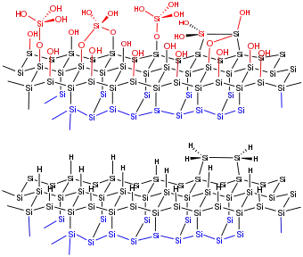
Hydrogen-terminated silicon surface is a chemically passivated silicon substrate where the surface Si atoms are bonded to hydrogen.[1] The hydrogen-terminated surfaces are hydrophobic, luminescent, and amenable to chemical modification.[2] Hydrogen-terminated silicon is an intermediate in the growth of bulk silicon from silane:[3]
- SiH4 → Si + 2 H2
Preparation

Silicon wafers are treated with solutions of electronic-grade hydrofluoric acid in water, buffered water, or alcohol. One of the relevant reactions is simply removal of silicon oxides:
- SiO2 + 4 HF → SiF4 + 2 H2O
The key reaction however is the formation of the hydrosilane functional group.
atomic force microscope (AFM) has been used to manipulate hydrogen-terminated silicon surfaces.[4][5]
Properties

Hydrogen termination removes dangling bonds. All surface Si atoms are tetrahedral. Hydrogen termination confers stability in ambient environments. So again, the surface is both clean (of oxides) and relatively inert. These materials can be handled in air without special care for several minutes.[6]
The Si-H bond in fact is stronger than the Si-Si bonds. Two kinds of Si-H centers are proposed, both featuring terminal Si-H bonds. One kind of site has one Si-H bond. The other kind of site features SiH2 centers.[3]
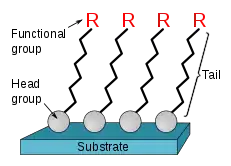
Like organic hydrosilanes, the H-Si groups on the surface react with terminal alkenes and diazo groups. The reaction is called hydrosilylation. Many kinds of organic compounds with various functions can be introduced onto the silicon surface by the hydrosilylation of a hydrogen-terminated surface. The infrared spectrum of hydrogen-terminated silicon shows a band near 2090 cm−1, not very different from νSi-H for organic hydrosilanes.[6]
Potential applications
One group proposed to use the material to create digital circuits made of quantum dots by removing hydrogen atoms from the silicon surface.[4]
See also
References
- ↑ Fenner, D. B.; Biegelsen, D. K.; Bringans, R. D. (1989). "Silicon surface passivation by hydrogen termination: A comparative study of preparation methods". Journal of Applied Physics. 66 (1): 419–424. Bibcode:1989JAP....66..419F. doi:10.1063/1.343839.
- ↑ Lauerhaas, Jeffrey M.; Sailor, Michael J. (1993). "Chemical Modification of the Photoluminescence Quenching of Porous Silicon". Science. 261 (5128): 1567–1568. Bibcode:1993Sci...261.1567L. doi:10.1126/science.261.5128.1567. PMID 17798116. S2CID 12722221.
- 1 2 Waltenburg, Hanne Neergaard; Yates, John (1995). "Surface Chemistry of Silicon". Chem. Rev. 95: 1589–1673. doi:10.1021/cr00037a600.
- 1 2 "Manipulating silicon atoms to create future ultra-fast, ultra-low-power chip technology". www.kurzweilai.net. 2017-02-17. Retrieved 2017-02-22.
- ↑ Labidi, Hatem; Koleini, Mohammad; Huff, Taleana; Salomons, Mark; Cloutier, Martin; Pitters, Jason; Wolkow, Robert A. (2017-02-13). "Indications of chemical bond contrast in AFM images of a hydrogen-terminated silicon surface". Nature Communications. 8: 14222. Bibcode:2017NatCo...814222L. doi:10.1038/ncomms14222. ISSN 2041-1723. PMC 5316802. PMID 28194036.
- 1 2 "Organic modification of hydrogen terminated silicon surfaces1". Journal of the Chemical Society, Perkin Transactions 2: 23–34. 2002. doi:10.1039/B100704L.
External links
- UAlbertaScience (2016-10-31), Less is more for atomic-scale manufacturing, archived from the original on 2021-12-13, retrieved 2017-02-22
- UAlbertaScience (2017-02-13), Patterning and imaging electronic circuits at the atomic level, archived from the original on 2021-12-13, retrieved 2017-02-22