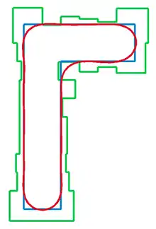
In semiconductor device fabrication, the inverse lithography technology (ILT) is an approach to photomask design. This is basically an approach to solve an inverse imaging problem: to calculate the shapes of the openings in a photomask ("source") so that the passing light produces a good approximation of the desired pattern ("target") on the illuminated material, typically a photoresist. As such, it is treated as a mathematical optimization problem of a special kind, because usually an analytical solution does not exist.[1] In conventional approaches known as the optical proximity correction (OPC) a "target" shape is augmented with carefully tuned rectangles to produce a "Manhattan shape" for the "source", as shown in the illustration. The ILT approach generates curvilinear shapes for the "source", which deliver better approximations for the "target".[2]
The ILT was proposed in 1980s, however at that time it was impractical due to the huge required computational power and complicated "source" shapes, which presented difficulties for verification (design rule checking) and manufacturing. However in late 2000s developers started reconsidering ILT due to significant increases in computational power.[1]
References
- 1 2 S. Chan; A. Wong; E. Lam (2008), "Initialization for robust inverse synthesis of phase-shifting masks in optical projection lithography", Optics Express, 16 (19): 14746–14760, Bibcode:2008OExpr..1614746C, doi:10.1364/OE.16.014746, PMID 18795012
- ↑ Inverse Lithography Technology (ILT)