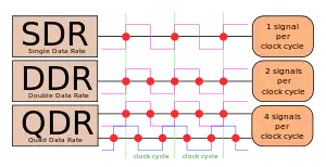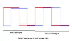

Quad data rate (QDR, or quad pumping) is a communication signaling technique wherein data are transmitted at four points in the clock cycle: on the rising and falling edges, and at two intermediate points between them. The intermediate points are defined by a second clock that is 90° out of phase from the first. The effect is to deliver four bits of data per signal line per clock cycle.[1]
In a quad data rate system, the data lines operate at twice the frequency of the clock signal. This is in contrast to double data rate systems, in which the clock and data lines operate at the same frequency.[1]
Quad data rate technology was introduced by Intel in its Willamette-core Pentium 4 processor, and was subsequently employed in its Atom, Pentium 4, Celeron, Pentium D and Core 2 processor ranges. This technology has allowed Intel to produce chipsets and processors that can communicate with each other at data rates expected of the traditional front-side bus (FSB) technology running from 400 MT/s to 1600 MT/s, while maintaining a lower and thus more stable actual clock frequency of 100 MHz to 400 MHz.[2]
Background
The reasons for operating in QDR rather than DDR are very different than those cited for operating in DDR rather than single data rate. Going to DDR allowed manufacturers of memory to send data at the same rate as the clock beat (one data-line transition for every clock-line transition), while SDR could only send data at the rate of the clock cycle (one data-line transition for every clock-line rising edge). A naive implementation of QDR would result in the data rate being higher than the clock rate, negating any simple electrical advantage.
The advantages for QDR arise when dealing with bus contention. On a modern computer, there may be several CPUs and several I/O devices, all competing for accesses to the memory. To handle this contention properly, modern systems aim to enable signals to propagate between all connected components within a single clock cycle, while setting a firm limit on the maximum clock rate. However, once the contention has been dealt with, the data transfer can be treated as a simple point-to-point unidirectional transfer. In such a simple transfer, it is no longer essential for signals to fully propagate within a cycle; they merely need to arrive coherently, marshaled by a special signal called "strobe". This reduced requirement on signal integrity allows the QDR data transfer to occur at twice the speed of the clock, as opposed to at the same speed as the clock as in DDR.[3]
See also
References
- 1 2 Lee Penrod (2007-08-21). "Understanding System Memory and CPU speeds: A layman's guide to the Front Side Bus (FSB)". directron.com. Archived from the original on 2016-01-18. Retrieved 2015-01-30.
- ↑ Thomas Soderstrom (2006-07-26). "Quad Data Rate Northbridge Technologies (S478, S775)". tomshardware.com. Retrieved 2014-01-09.
- ↑ Intel (2004-10-19). "Patent US6807592". Retrieved 2014-09-08.