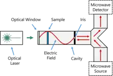
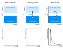
Time resolved microwave conductivity (TRMC) is an experimental technique used to evaluate the electronic properties of semiconductors. Specifically, it is used to evaluate a proxy for charge carrier mobility and a representative carrier lifetime from light-induced changes in conductance. The technique works by photo-generating electrons and holes in a semiconductor, allowing these charge carriers to move under a microwave field, and detecting the resulting changes in the electric field. TRMC systems cannot be purchased as a single unit, and are generally "home-built" from individual components. One advantage of TRMC over alternative techniques is that it does not require direct physical contact to the material.
History

While semiconductors have been studied using microwave radiation since the 1950s,[1] it was not until the late 1970s and early 1980s that John Warman at the Delft University of Technology exploited microwaves for time-resolved measurements of photoconductivity. The first reports used electrons[2] then photons[3] to generate charges in fluids. The technique was later refined to study semiconductors by Kunst and Beck at the Hahn Meitner Institute in Berlin.[4]
Delft remains a significant center for TRMC,[5] however the technique is now used at a number of institutions around the world, notably the National Renewable Energy Laboratory[6] and Kyoto University.[7]
Operating principles
The experiment relies upon the interaction between optically-generated charge carriers and microwave frequency electromagnetic radiation. The most common approach is to use a resonant cavity.[8] An oscillating voltage is produced using a signal generator such as a voltage controlled oscillator or a Gunn diode. The oscillating current is incident on an antenna, resulting in the emission of microwaves of the same frequency. These microwaves are then directed into a resonant cavity. Because they can transmit microwaves with lower loss than cables,[9] metallic waveguides are often used to form the circuit.[10] With the appropriate cavity dimensions and microwave frequency, a standing wave can be formed with 1 full wavelength filing the cavity.

The sample to be studied is placed at a maximum of the electric field component of the standing wave. Because metals act as cavity walls,[9] the sample needs to have a relatively low free carrier concentration in the dark to be measurable. TRMC is hence best suited to the study of intrinsic or lightly doped semiconductors. Electrons and hole are generated by illuminating the sample with above band gap optical photons. Optical access to the sample is provided by a cavity wall which is both electrically conducting and optically transparent; for example a metallic grating or a transparent conducting oxide.
The photo-generated charge carriers move under the influence of the electric field component of the standing wave, resulting in a change in intensity of microwaves that leave the cavity. The intensity of microwaves out of the cavity is measured as a function of time using an appropriate detector and an oscilloscope. Knowledge of the properties of the cavity can be used[8] to evaluate photoconductance from changes in microwave intensity.
Theory

The reflection coefficient is determined by the coupling between cavity and waveguide.[11] When the frequency of microwave is resonant frequency, the reflectance, , of the cavity is expressed as follows:
Here is the quality factor of the cavity including the sample, is the quality factor of the external coupling, which is generally adjusted by iris. The total loaded quality factor of the cavity, , is defined as follows:
The photo-generated charge carriers reduce the quality of the cavity, . When the change of quality factor is very small, the change of reflected microwave power is approximately proportional to the change of dissipation factor of the cavity. Furthermore, dissipation factor of the cavity is mainly determined by the conductivity of the inside space including the sample. Consequently, the change in the conductivity, , of the cavity contents is proportional to relative changes in microwave intensity:[2]
Here is the background (unperturbed) microwave power measured coming out of the cavity and is the change in microwave power as a result of the change in cavity conductance. is the sensitivity factor determined by the quality of the cavity, is the geometry factor of the sample. can be derived by Taylor expanding of the reflectance equation:
Here is the resonant frequency of the cavity in Hertz unit, is the vacuum permittivity, is the relative permittivity of the medium inside the cavity. The relative permittivity should be considered only when the cavity is filled by solvent. When the sample is inserted into dry cavity, only vacuum permittivity should be used because most of the inside space is filled by air. The sign of depends on whether the cavity is in the under-coupled (lower) or over-coupled (upper) regime. So, the negative signal is detected in over-coupled regime, , whereas the positive signal is detected in under-coupled regime, . No signal can be detected at critical coupling condition,
is determined by the overlap between the electric field and the sample position:[10]
Here is the electric field in the cavity. and denote the total inside volume of the cavity and the volume of photo-generated carriers, respectively. If the thickness of the sample is sufficiently thin (below several μm), the electric field to photo-generated carriers would be uniform. In this condition, is approximately proportional to the thickness of the sample. Above conductivity equation can be expressed as follows:
Here is the elementary charge, is the transmittance of the sample at the excitation wavelength, is the incident laser fluence, is the quantum yield of photo-carrier generation per absorbed photon, is the sum of the electron and hole mobility, is the thickness of the sample. Because is linearly proportional to the thickness, only the fractional absorbance of the semiconductor (between 0 and 1) should be additionally measured to determine the TRMC figure of merit (e.g. using ultraviolet–visible spectroscopy):
Applications
Knowledge of charge carrier mobility in semiconductors is important for understanding the electronic and materials properties of a system. It is also valuable in device design and optimization. This is particularly true for thin film solar cells and thin film transistors, where charge extraction[12] and amplification,[13] respectively, are highly dependent upon mobility. TRMC has been used to study electron and hole dynamics in hydrogenated amorphous silicon,[14] organic semiconductors,[15] metal halide perovskites,[16] metal oxides,[17] dye sensitized systems,[18] quantum dots,[19] carbon nanotubes,[20] chalcogenides,[21] metal organic frameworks,[22] and the interfaces between various systems.[23]
Because charges are normally generated using a green (~2.3 eV) or ultraviolet (~3 eV) laser, this restricts materials to those with comparable or smaller bandgaps. The technique is hence well suited to the study of solar absorbers, but not to wide bandgap semiconductors such as metal oxides.
While it is very similar, and has the same dimensions, the parameter is not the same a charge carrier mobility. contains contributions from both holes and electrons, which cannot conventionally be resolved using TRMC. This is in contrast to Hall Measurements or transistor measurements, where hole and electron mobility can easily be separated. Additionally, the mobility is not directly extracted from the measurements, it is measured multiplied by the carrier generation yield, . The carrier generation yield is the number of electron hole pairs generated per absorbed photon. Because some absorbed photons can lead to bound neutral excitons, not all absorbed photons will lead to detectable free carriers. This can make interpretation of more complicated than mobility. However, generally both mobility and are parameters which one wishes to maximize when developing solar cells.
As a time-resolved technique, TRMC also provides information on the timescale of carrier recombination in solar cells. Unlike time resolved photoluminescence measurements, TRMC is not sensitive to the lifetime of excitons.
See also
References
- ↑ Gibson, A. F. (1956). "The Absorption of 39 kMc/s (39 Gc/s) Radiation in Germanium". Proceedings of the Physical Society. Section B. 69 (4): 488–490. doi:10.1088/0370-1301/69/4/111.
- 1 2 Infelta, Pierre P.; De Haas, Matthijs P.; Warman, John M. (1977). "The study of the transient conductivity of pulse irradiated dielectric liquids on a nanosecond timescale using microwaves". Radiation Physics and Chemistry (1977). 10 (5–6): 353–365. Bibcode:1977RaPC...10..353I. doi:10.1016/0146-5724(77)90044-9.
- ↑ De Haas, Matthijs P.; Warman, John M. (1982). "Photon-induced molecular charge separation studied by nanosecond time-resolved microwave conductivity". Chemical Physics. 73 (1–2): 35–53. Bibcode:1982CP.....73...35D. doi:10.1016/0301-0104(82)85148-3.
- ↑ Kunst, M.; Beck, G. (1986). "The study of charge carrier kinetics in semiconductors by microwave conductivity measurements". Journal of Applied Physics. 60 (10): 3558–3566. Bibcode:1986JAP....60.3558K. doi:10.1063/1.337612.
- ↑ "TRMC". TU Delft. Retrieved 2021-08-21.
- ↑ "Garry Rumbles". www.nrel.gov. Retrieved 2021-08-21.
- ↑ "SEKI Lab. | Researches". www.moleng.kyoto-u.ac.jp. Retrieved 2021-08-21.
- 1 2 Savenije, Tom J.; Ferguson, Andrew J.; Kopidakis, Nikos; Rumbles, Garry (2013). "Revealing the Dynamics of Charge Carriers in Polymer:Fullerene Blends Using Photoinduced Time-Resolved Microwave Conductivity". The Journal of Physical Chemistry C. 117 (46): 24085–24103. doi:10.1021/jp406706u.
- 1 2 Feynman, Richard P.; Leighton, Robert B.; Sands, Matthew (2015). The Feynman Lectures on Physics, Vol. II: The New Millennium Edition: Mainly Electromagnetism and Matter. Basic Books. ISBN 978-0-465-04084-1.
- 1 2 Saeki, A.; Seki, S.; Sunagawa, T.; Ushida, K.; Tagawa, S. (2006). "Charge-carrier dynamics in polythiophene films studied by in-situ measurement of flash-photolysis time-resolved microwave conductivity (FP-TRMC) and transient optical spectroscopy (TOS)". Philosophical Magazine. 86 (9): 1261–1276. Bibcode:2006PMag...86.1261S. doi:10.1080/14786430500380159. S2CID 95219747.
- ↑ Tomonaga, S. (1948). "A general Theory of Ultra-short Wave Circuits". Journal of the Physical Society of Japan. 2 (2–3): 93–105. doi:10.1143/JPSJ.3.93.
- ↑ Nelson, Jenny (2003-01-01). The Physics of Solar Cells. Imperial College Press. ISBN 978-1-86094-349-2.
- ↑ Brotherton, S. D. (2013). Introduction to Thin Film Transistors: Physics and Technology of TFTs. Springer International Publishing. ISBN 978-3-319-00001-5.
- ↑ Kunst, M.; Werner, A. (1985). "Comparative study of time-resolved conductivity measurements in hydrogenated amorphous silicon". Journal of Applied Physics. 58 (6): 2236–2241. Bibcode:1985JAP....58.2236K. doi:10.1063/1.335940.
- ↑ Dicker, Gerald; de Haas, Matthijs P.; Siebbeles, Laurens D.A.; Warman, John M. (2004). "Electrodeless time-resolved microwave conductivity study of charge-carrier photogeneration in regioregular poly(3-hexylthiophene) thin films". Physical Review B. 70 (4): 045203. Bibcode:2004PhRvB..70d5203D. doi:10.1103/PhysRevB.70.045203.
- ↑ Oga, Hikaru; Saeki, Akinori; Ogomi, Yuhei; Hayase, Shuzi; Seki, Shu (2014). "Improved Understanding of the Electronic and Energetic Landscapes of Perovskite Solar Cells: High Local Charge Carrier Mobility, Reduced Recombination, and Extremely Shallow Traps". Journal of the American Chemical Society. 136 (39): 13818–13825. doi:10.1021/ja506936f. PMID 25188538.
- ↑ Abdi, Fatwa F.; Savenije, Tom J.; May, Matthias M.; Dam, Bernard; van de Krol, Roel (2013). "The Origin of Slow Carrier Transport in BiVO4 Thin Film Photoanodes: A Time-Resolved Microwave Conductivity Study". The Journal of Physical Chemistry Letters. 4 (16): 2752–2757. doi:10.1021/jz4013257.
- ↑ Friedrich, Dennis; Kunst, Marinus (2011). "Analysis of Charge Carrier Kinetics in Nanoporous Systems by Time Resolved Photoconductance Measurements". The Journal of Physical Chemistry C. 115 (33): 16657–16663. doi:10.1021/jp200742z.
- ↑ Straus, Daniel B.; Goodwin, E. D.; Gaulding, E. Ashley; Muramoto, Shin; Murray, Christopher B.; Kagan, Cherie R. (2015). "Increased Carrier Mobility and Lifetime in CdSe Quantum Dot Thin Films through Surface Trap Passivation and Doping". The Journal of Physical Chemistry Letters. 6 (22): 4605–4609. doi:10.1021/acs.jpclett.5b02251. PMID 26536065.
- ↑ Park, Jaehong; Reid, Obadiah G.; Blackburn, Jeffrey L.; Rumbles, Garry (2015). "Photoinduced spontaneous free-carrier generation in semiconducting single-walled carbon nanotubes". Nature Communications. 6 (1): 8809. Bibcode:2015NatCo...6.8809P. doi:10.1038/ncomms9809. PMC 4667683. PMID 26531728.
- ↑ Savenije, Tom J.; Nanu, Marian; Schoonman, Joop; Goossens, Albert (2007). "A time-resolved microwave conductivity study of the optoelectronic processes in TiO2∣In2S3∣CuInS2 heterojunctions". Journal of Applied Physics. 101 (11): 113718–113718–7. Bibcode:2007JAP...101k3718S. doi:10.1063/1.2745386.
- ↑ Dolgopolova, Ekaterina A.; Brandt, Amy J.; Ejegbavwo, Otega A.; Duke, Audrey S.; Maddumapatabandi, Thathsara D.; Galhenage, Randima P.; Larson, Bryon W.; Reid, Obadiah G.; Ammal, Salai C.; Heyden, Andreas; Chandrashekhar, Mvs (2017). "Electronic Properties of Bimetallic Metal–Organic Frameworks (MOFs): Tailoring the Density of Electronic States through MOF Modularity". Journal of the American Chemical Society. 139 (14): 5201–5209. doi:10.1021/jacs.7b01125. OSTI 1352137. PMID 28316244.
- ↑ Hutter, Eline M.; Hofman, Jan-Jaap; Petrus, Michiel L.; Moes, Michiel; Abellón, Ruben D.; Docampo, Pablo; Savenije, Tom J. (2017). "Charge Transfer from Methylammonium Lead Iodide Perovskite to Organic Transport Materials: Efficiencies, Transfer Rates, and Interfacial Recombination". Advanced Energy Materials. 7 (13): 1602349. Bibcode:2017AdEnM...702349H. doi:10.1002/aenm.201602349. S2CID 99733680.